Table of Contents
- What is DDS or NCO… 3
- Performance parameter of NCO-SFDR, MSE, Power, step size.. 4
- Block Diagram and Summary Table of SoulRA NCO… 4
- FPGA resources of SoulRA NCO-Lattice.. 15
- FPGA resources of SoulRA NCO-Xilinx. 16
- Dynamic Power Requirements for various SoulRA NCO… 17
- SFDR plots of SoulRA NCO… 18
- NCO Control Interfaces. 21
- NCO frequency step size control 21
- NCO phase control 22
- Matlab models for SoulRa NCO… 22
- Support: 22
Section 1
What is DDS or NCO
Section 2
Performance parameter of NCO-SFDR, MSE, Power, step size
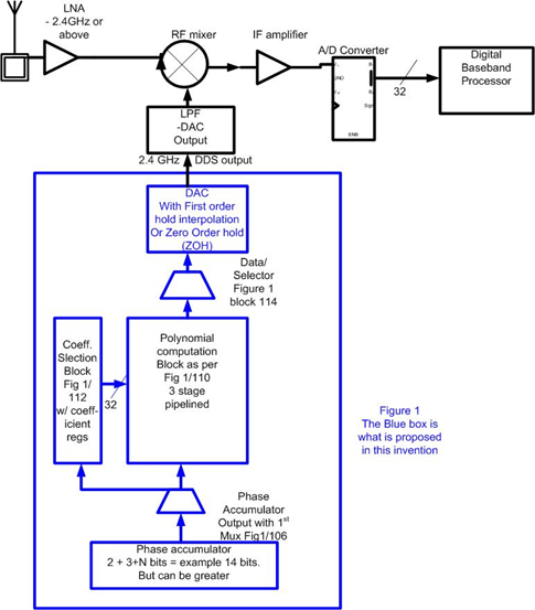
The DDS or NCO block is illustrated in Figure 1- it is a device designed to synthesize waveforms. It comprises of three sub blocks – the phase accumulator block which generates a digital phase word corresponding to a phase between 0 and 360o. The output of the phase accumulator block feeds a Polynomial Computation Block which is a 3 or 4 stage pipeline with only adders and multipliers and interstage registers.
The final block (Figure 1) is a coefficient selection block which generates the coefficients corresponding to various segments of a Quadrant. Each Quadrant is subdivided into a power of 2 number of segments eg. 8, 16, 32, 64 ….
The output of the polynomial block is scaled so that it can directly drive a DAC. In the example in Figure 1. The DAC output is shown driving a down conversion Mixer of a Cognitive Radio.
Block Diagram and Summary Table of SoulRA NCO
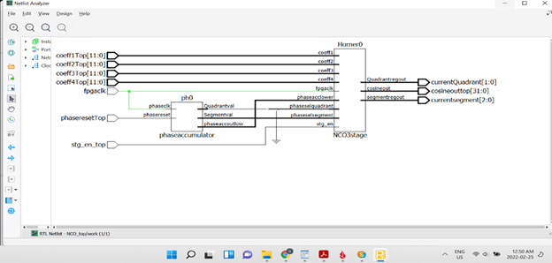
This NCO consists of 6 major blocks (Figure 2). The first block (106) is the phase accumulator. The phase accumulator (106) generates a value of phase between 0 and 2π based on a reference clock. The phase accumulator output drives the multiplexer block (107). In figure 2 a 12-bit output of the phase accumulator is shown. The lower 12 bits of the phase accumulator output corresponds to 4096 samples which covers one quadrant of a waveform. More details pertaining to the phase accumulator are given in the General Background section. The phase accumulator output is split into 4 subfields. The uppermost bit selects between the positive and negative half cycle, the next significant bit between odd and even quadrant.
The next 3 bits select one sector out of 8 sectors in each quadrant (termed “s” hereafter).
The last 9 bits are for fine increments of angle- 9 bits make a possible 512 samples within each sector. In this wave a full wave is split into 4 quadrants and each quadrant into further 8 sectors and each sector has 512 fine phase increments. Fig 2A and 2B in General Background explain this in detail. In example implementation in Fig 6 of the General background section shows 16K samples for a full cycle. Figure 2 shows the connectivity of various blocks of the NCO. There are 3 major blocks and 2 additional MUXes in Figure 2.
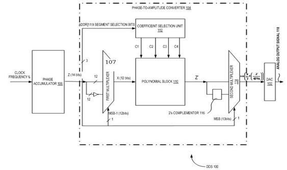
The second block (Figure 2) is a selection block (“First Multiplexer”) which selects between the phase value and its complement. The output of the “First Multiplexer” block is fed to the Polynomial block-110. The primary task of the second block is to select between odd-quadrants and even quadrants.
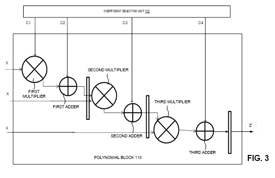
The third block in the system is the polynomial block (110). This is further detailed in Figure 3. The core of the computation is performed by a 3-stage pipelined polynomial block (110). The polynomial block computes the output value for a given segment and given phase angle. It uses Horner’s rule to reduce the number of total multiplications from 6 to 3 multiplications per output sample. The critical path is reduced from (6Tm + 3Ta) to (Tm + Ta) which is a 8 fold reduction in the critical path- for 65nm process this corresponds to a critical path delay of 3ns. The details of the polynomial sub-block are given in the fig 3 of the General background section. The output of the polynomial block corresponds to a single half cycle. The reduction of the critical path is a major feature of this invention.
The fourth block stores 32 hard coded coefficients 4 for each quadrant of the sine wave (Coefficient selection unit no. 112). The bits [11:9] 3 bits are used to select one of 8 segments. The fourth block is a selection block which supplies the required coefficients for the cubic polynomial. The internal sub-blocks are discussed in Fig 4A in the General Background section.
The fifth block is the selector or second multiplexer block (114) which selects between positive and negative half cycles. The topmost bit of the phase accumulator is used to make the selection [bit 14 in this example]. This block acts as a high-speed multiplexer. Its output is digital and the bit-width is the same as the input of a DAC. The width of this block controls the level of SNR due to amplitude truncation.
The sixth block is the digital to analogue conversion block (102). The DAC can be zero order hold (ZOH) or it is better first order hold interpolation DAC (FOHI DAC). This specific invention calls for a first order hold with interpolation DAC which provides a much smoother output than a ZOH(Zero-order-hold) DAC. The DAC will be located in the same or a different silicon die.
The next bits of the phase accumulator output are used to select one of 8 segments in the coefficient selection unit (112). Corresponding to each segment the coefficient selection unit generates 4 coefficients. The 4 coefficients can be generated in a multiplicity of formats like 2’s complement, sign-magnitude, Gray coded etc. Floating point formats as per IEEE754 can be used. The demonstration model in fig 6 and fig 4A shows fixed point formats. The advantage of the approach is only 32 hard-wired registers need to be used to generate all required coefficients. Comparatively a conventional ROM based DDS would require 16L locations of a minimum of 4 bytes for a ROM size of 64 K.
The core of the computation is performed by a 3-stage pipelined polynomial block (110). The polynomial block computes the output value for a given segment and given phase angle. It uses Horner’s rule to reduce the number of total multiplications from 6 to 3 multiplications per output sample. The critical path is reduced from (6Tm + 3Ta) to (Tm + Ta) which is a 8 fold reduction in the critical path. The details of the polynomial sub-block are given in the fig 3 of the General background section. The output of the polynomial block corresponds to a single half cycle.
The final block is the selector block which selects between positive and negative half cycles. The topmost bit of the phase accumulator is used to make the selection.
The final digital output of the NCO is sent to a DAC which is outside the FPGA IP.
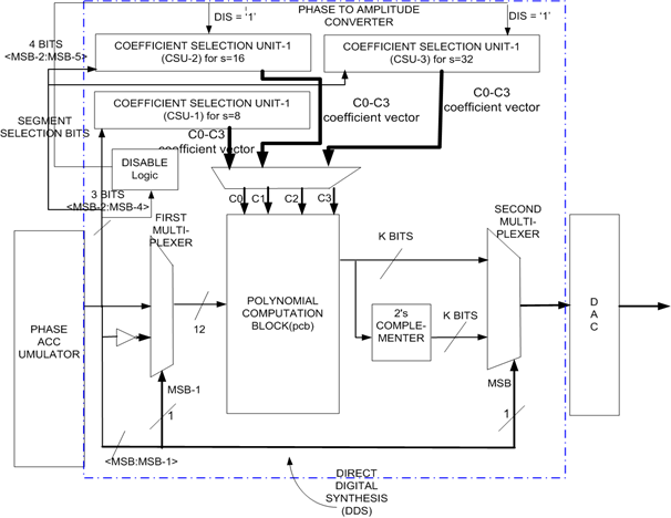
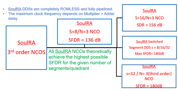
Figure 3 comprises of a key pipeline – the first block is a Phase accumulator which generates the phase word which generates a phase word 2+(M bits) + N bits. The top two bits are used to select one of four Quadrants. The next M bits with M = 3/4/5 are used to select between 8/16/32 segments. The lowest N bits are used to select between the number of samples per segment, in the default this is 12 bits per segment which means the phase accumulator width is (2+3+12= 17 bits for 8 segments (SFDR=136dB). Or (2+4+12= 18 bits for 16 segments/quadrant (sFDR-160dB) or (2+5+12 = 19 bits for 32 segments / quadrant (SFDR=180dB).
The first block is a multiplexer (Mux) that selects between the phase word and its binary complement. The COEFF registers are hard coded registers which are banked into three banks- CSU-1 (8 segments a total of 4×8 registers.). The second coefficient selection unit CSU-2 selects coefficients for 16 segments – a total of 16×8 registers.
The polynomial block is a three-stage pipeline to compute the Final NCO output. Description of the Polynomial Block follows.
FIG. 4 illustrates a circuit diagram of the polynomial block. The polynomial block 110 includes a first multiplier, a first adder, a second multiplier, a second adder, a third multiplier, and a third adder. The first multiplier is coupled to the first adder, a first adder is coupled to the second multiplier. The second multiplier is coupled to the second adder. The second adder

In one exemplary operation, the first multiplier receives X [11:0 bits] as input from the first multiplexer 108- (Figure 3). The first multiplier also receives a constant C1 associated with a segment (indicated by segment selection bits [11:9]) of the selected quadrant from the coefficient selection module 112. The output of the first multiplier is coupled to the first adder which adds with the constant C2 associated with said segment of the selected quadrant from the coefficient selection module 112. The output of the first adder is provided to the second multiplier, via a first register, to generate an output by multiplying the output from the second adder and the value X.
The output of the second multiplier is then provided to the second adder which adds the multiplier output with the constant C3 associated with said segment of the selected quadrant from the coefficient selection module 112. The output of the second adder is fed to the third multiplier via a second register to generate an output by multiplying the value X and output of the second adder.
The third multiplier output is fed to the third adder which adds the multiplier output with the constant C4 associated with said segment of the selected quadrant to


The two performance parameters for NCOs are SFDR and MAE,
SFDR definition for Cubic DDS : SFDR as a function of the number of segments can be written as
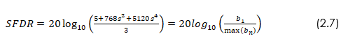
In the Equation 2 the SFDR is expressed as a function of the number of segments /quadrant.

In Equation (4), the DDS_out is estimated by a cubic polynomial represented through Equation (2.14). Its is the difference between the DDS/NCO output and an ideal sinusoid.
MAE Plot for segment = 8 Cubic DDS.
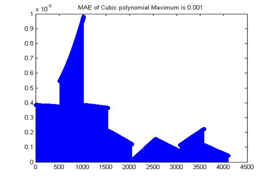
In figure 5 The MAE is computed over and entire Quadrant ie. 512*8 = 4096 samples. The peak MAE is under 10^-3. The MAE is defined as Maximum Absolute Error.
MAE is used as the second performance parameter in this IP description after SFDR. In the second figure we look at a spectral picture of the NCO output.
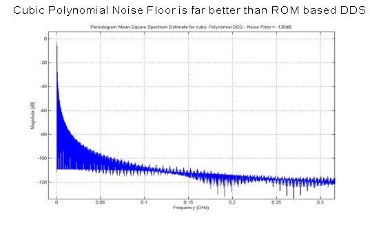
FIG. 6 is a periodogram obtained from the signal (W) at the output of the phase to amplitude converter or NCO. In one aspect, the periodogram indicates the primary signal output, along with the unwanted spurs and displays a noise floor associated with the cubic polynomial DDS 100 of FIGS. 1 and 6. FIG. 7 shows that, the noise floor associated with the DDS 100 is -120db which is much better than the ROM based DDS (having a noise floor of -76db to -90db). This is a significant improvement made in the proposed DDS 100. This occurs along with power savings (consumed by the ROMs in the conventional DDS). The low noise floor of the NCO allows a better sinusoid at the input of the DAC 102. This leads to a cleaner signal at the output of the DAC 102. This is turn leads to better signal at the mixer input and better mixer performance and better overall receiver performance (Fig 1).
Table1: Summary of SoulRA NCO features:
| SFDR | 136 dB ( 8 segment ); 156 dB( 16 segment ) and 180dB ( 32 segment/Quadrant) |
| Frequency Step Size | 3 stage pipeline – Cubic Polynomial; 4 stage – Quartic DDS;2 stage pipeline -LHSC DDS |
| Phase accumulator bit width | 17/18/19 |
| Quadratic output, sin and cos available | Yes for all DDS Sine and Cosine outputs are available |
| SFDR adjustable or not | SFDR is adjustable using altered number of segments – 136dB (8 segments / Quadrant) ; 156 dB( 16 Segments / Quadrant) ; 180 dB (32 Segments / Quadrant). LHSC DDS with 32 = 180 dB (SFDR) |
| Implementation | ASIC or FPGA – Verilog Code |
| LUT Count on Lattice | Registers = 38 ++; LUT4=20++; Multiplier=4; Accumulator=3++; |
| Matlab Model | Available |
| Dithering options | Phase Dithering available |
Part 6: DDS(NCO) dynamic power requirement
DDS dynamic power expressed as a normalized value.
Unit or 100 is Cubic DDS with 8 segments/quadrant.
Section 4
FPGA resources of SoulRA NCO-Lattice
Section 5
FPGA resources of SoulRA NCO-Xilinx
Table 2
| Type of FPGA circuit elements used | Absolute FPGA resources used | Percentage of FPGA resources for Virtex-6 |
| Number of Slice registers | 1852 | 1% |
| Number of Slide LUTs | 2792 | 1% |
| Number of LUTs used as Logic | 1901 | 1% |
| Number of LUTs used as memory | 517 | 2% |
| Number of LUT-FF pairs | 3090 | 45% |
Section 6
Dynamic Power Requirements for various SoulRA NCO
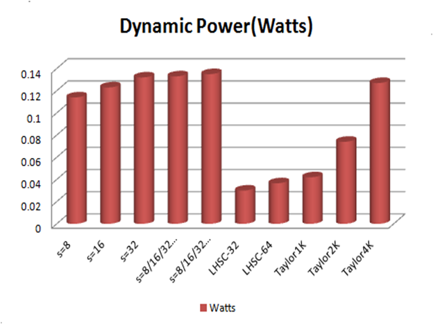
The power requirement values are plotted for various configurations of the DDS. The first column is for Cubic DDS with a 3-stage pipeline and s=8(8 segments/Quadrant). The second bar is for 16 segments / quadrant, the third bar is for 32 segments/quadrant. The next two bars are for a switchable DDS with variable number of segments and N= 512 or 1024. The last five bars are for non-Cubic DDS and outside the scope of this datasheet.
The second plot is for SFDR – Spurious Free Dynamic Range. The SFDR is the most important performance measure for any NCO.
Section 7
SFDR plots of SoulRA NCO
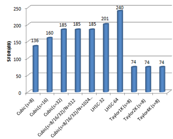
The first three curves are of interest here, they correspond to s=8/16/32 or rather segments / quadrant varying from 8 through 32. The next two bars are for switchable DDS and its clear the SFDR is only a function of segments/quadrant.
It is observed the maximum achievable SFDR is 180dB.
The SoulRA Cubic polynomial offerings are combined into a single graphic in Figure 11.
The current design of the NCO allows dynamic switching of SFDR and the LUT complexity between the lowest SFDR configuration to the highest SFDR configuration is under 10%. The NCO design can be scaled to the high SFDR of 180dB with higher number of segments but the resultant increase in LUT count is under 10%. There are no additional multipliers or adders required to increase the SFDR.
Post Synthesis NCO:
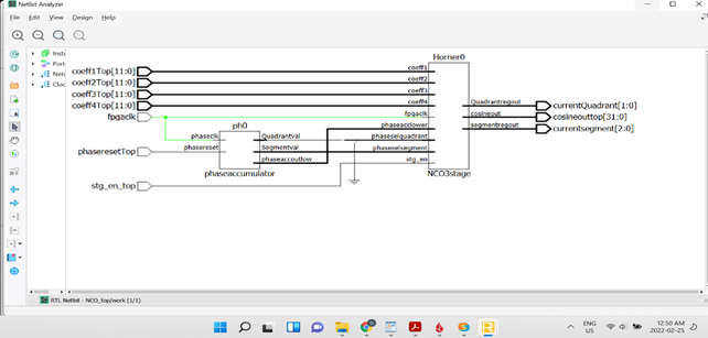
Table 3: Currently Supported FPGA families which can host the SoulRA NCO IP
| Lattice FPGAs | Certus NX, Certus Nx Pro |
| Xilinx FPGAs | Virtex-7 Virtex-6, Kintex-7, Artix-7 |
| Intel FPGAs | All Cyclone, Spartan series of FPGAs Stratix FPGAs, |
Section 8
NCO Control Interfaces
The NCO Control Interfaces can set the SFDR value by altering the number of number of segments per quadrant. The second control mechanism alters the number of bits of phase word which in turn controls the samples per segment.
Table 4:The Two registers that are used to control are described in this table.
| Register1 | 00: s= 8 ( 8 segments / quadrant); 01 : s=16 ( 16 segments/quadrant); 10: s=32 ( 16 segments /quadrant) |
| Register 2 | 00: 256 samples/segment: 01: 512 samples/segment |
Section 9
NCO frequency step size control
The frequency Step size control is activated by register 3 which is programmed with one of four values, it allows the selection of one of four primary blocks via register 3.
Table 5
| Register_Freq | Value and function |
| Value = 2’b00 | Output Frequency = fclk/N |
| Value = 2’b01 | Output Frequency = fclk/2N |
| Value = 2’b10 | Output Frequency = flck/3N |
| Value = 2’b11 | Output Frequency = fclk/4N |
Section 10
NCO phase control
The phase shift of the phase accumulator can be controlled by 8 fixed steps. Extended
Table 6
| Register_PhaseOffset | Value and function |
| Value = 3’b000 | Output Phase shift = pi/8 |
| Value = 3’b001 | Output Phase shift = pi/4 |
| Value = 3’b010 | Output Phase shift = 3*pi/8 |
| Value = 3’b011 | Output Frequency = pi/2 |
Section 11
MATLAB models for SoulRa NCO
Available: Example Plot is attached
Section 12
Support:
fpgasupport@soulra.net
Spondon@soulra.net